|
You
are
the visitor n.
Best view with 1024x768 |
||
|
You
are
the visitor n.
Best view with 1024x768 |
||
 |
 |
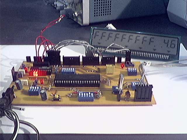
| The keypad and the Development Board v. 1.1 with a PIC 16F877 used to read it |
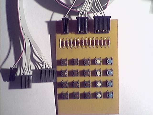
What's this? The circuit here described is a simple 4x5 keypad that can be used in particular with the PIC 16F877 microcontroller, for which it has been designed considering a supply of 5V, 16F877 I/O pins leakage current, the voltage level recognized as a high or low state while in TTL or ST mode, etc.. Since this circuit is quite simple, and the resistors' value not critical, it should be suitable for other PICs and other microcontrollers, too. This keypad can also be used with logic and analogue crcuits; in such a case, it could be necessary to modify resistors' value. We will refer, in this page, to the use with a PIC 16F877. The keys used are normally open, with four pins (see image below); when not pressed, only pins on the same side are connected together (left or right side in the image below); when the key is pressed, the four pins are connected all together. A characteristic of this circuit is the possibility of scaling: it can in fact be realized with 1 to 4 rows and 1 to 5 columns (if you still have free rows or columns, you can add later other keys and other resistors); you can build, as an example, a 12 keys telephonic keypad, a simple 4 keys keypad for the 4 directions, a keypad to play tris :-) ... in one word, what you like. The figure below shows
how it works (classic).
Driving columns and reading rows' state Referring to this keypad as an interface to a microcontroller (not necessarily a 16F877), the reading of keys' status is related to the matrix structure. As previously said, each key (or switch) has four pins, connected two by two; in the top view of the circuit (above here), the upper pin on the left is connected to a row, the upper one on the right to a column. The lower pin on the left is not used, the lower one on the right simply carries the column signal to the key of the next row. Let's consider a certain row: when no key connected to it is being pressed, all the row pins of that row are kept in the high state by the row pull-up; when a key is pressed, the column pin is connected to the row pin; if, in that moment, that column is in high impedance, it is driven at the row state; if it is instead driven low by the microcontroller, also the row is driven at the column state (low state). The microcontroller's ports connected to the rows must always be set as inputs, or, in general, must be kept in high impedance; in general, also the columns must be in high impedance. To read the state of the keys of a column, it is needed to drive low that column (only one) and to wait a few milliseconds both for the row's signal settling and to avoid the key's rebound; at this moment the column's state can be read on ports connected to rows. A suitable waiting time is five-ten milliseconds. As it is known which is the driven column, reading the rows' state it is possible to know the keys' status on that column. At this moment the pin driving that column must be put again in a high impedance state, and, possibly after a few milliseconds, a new column can be driven low and so on. Of course, it is not necessary to waist all this time in waiting: when waiting for settling, and in general among different readings, the microcontroller can execute (thousand of) other instructions. A typical way of reading keys' status could be using interrupts. As an example, in the PICs the timer could be set to generate an interrupt every a few tens milliseconds. A variable coding the action to take (action), and a variable keeping track of the column to read (coltoread) could be used. The first time that the interrupt routine is executed, it sees those two variables at zero (they should have been set to zero, of course): in such a case, the action to take is to drive low the column 0 and to increment the variable coding the action to take. When the next interrupt occurs, the interrupt driver sees such a variable at 1, so reads the rows' status for the column 0, puts it again in high impedance, increments the column number, set to 0 the variable coding the action to take. Of course, when the column number that has just been read is the highest for your keypad, the variable counting it (coltoread) must be set to 0. In a "pseudo" C++: void main( ) // interrupt routine Some remarks The logical state associated with pressed keys is low. When no column is driven (at low logical level), the state of pins driving columns, as they are in high impedance and not connected to any reference by a pull-up or pull-down, has no meaning: reading pins returns usually a time-variable state. When more than one key is pressed in the same column, the value read is correct. When more than one key is pressed in different columns, and there is no common row for pressed keys, the value read is correct. When more than one key is pressed in different columns, and there are common rows for pressed keys, reading columns whose keys have a common row returns the same result, so the global reading is wrong. The only true readings when more than one key is pressed in a column are those generated by pressing keys with no common rows. As an example, if we
think to keys as identified like elements of a 4 x 5 matrix, pressing
keys k11, k22, k31, k44 correctly generates the following reading (* =
key pressed, - = key not pressed):
Pressing keys k11, k31,
k32 generates instead the following wrong reading:
The method of reading a matrix keyboard is
obviously well known. The
project of the printed circuit board is entirely personal; an
acknowledgement goes to the software allowing me to realize the
circuit's layout. It is the program PCB Elegance v. 2.0; I have it in
the FREE version, limited to 200 pins, by MERCO Electronics, which has
authorized me by e-mail also to non-personal purposes. |
Components list All resistors are 1/4 W,
5%. R1, R2, R3, R4 - 47 KOhm Where can components be found? Components are quite standard, you should be able to find them in any electronic store. |
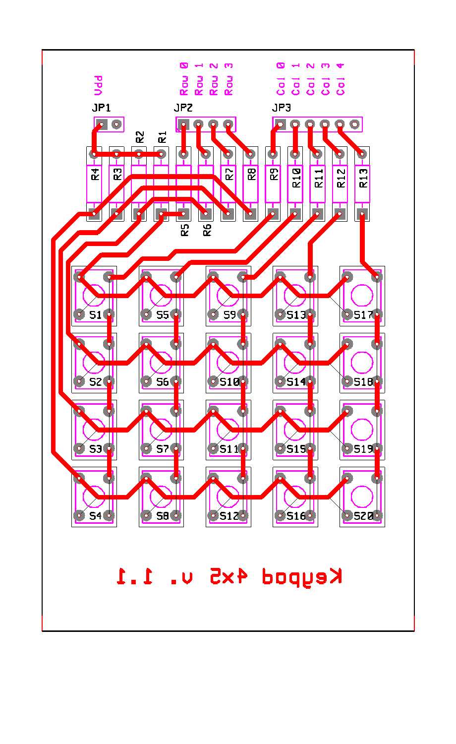
PCB layout printing You can see in the images below here the circuit's layout and how to place components. They are 100 or 300 dpi images. To obtain the same images, at 300 dpi, in a new window, from where you can print them or simply watch them enlarged, you just have to click on the images below or on the links under them, or, if you are using a Windows (TM) 95/98, you can use the right button and choose "Open link in new window". You can save the 300 dpi images on your hard disk or other media choosing "Save OBJECT with name" and print them later with your browser or other programs. With the browser you could have problems with the images' size, while, as an instance, Windows (TM) Imaging (TM) should print them in true size. If you are in doubt with regard to the size of the image you have printed, and you are in fear that it is not in true size, you can just measure the distance between holes for SIL components, which must be 2.54 mm between adjacent pins. Of course, not to make coarse mistakes, you could take as an example the distance between the first and the sixth pin, looking if it is 2.54 mm * (6-1) = 12.70 mm. You will not be able, of course, to measure hundredths of millimeters, and maybe not even tenths of millimeters (it would not be anyway very meaningful, given the size of pads and holes), but if your measure is a little bit more than 12.5 mm your printing should be good. To check the vertical scale, you could measure the distance between the two holes of a resistor; it must be 400 mils, that is 2.54 mm * 4 = 10.16 mm. If any of the two distances is not the one you are expecting, naming x that measure, you should apply a horizontal zoom factor of 12.70/x and a vertical zoom factor of 10.16/x. In figure 1 you could see the components' placement with the board looked at from top and against the light. You can see there that the bottom side layout (soldering side), when exposing the board to the light for the photoetching, must be placed with the printed side in contact with copper. Some of the images below are at low resolution, for obvious loading time reasons, but, as previously said, links on and under them allow you to see better resolution images and, in any case, enlarged ones. |
 |
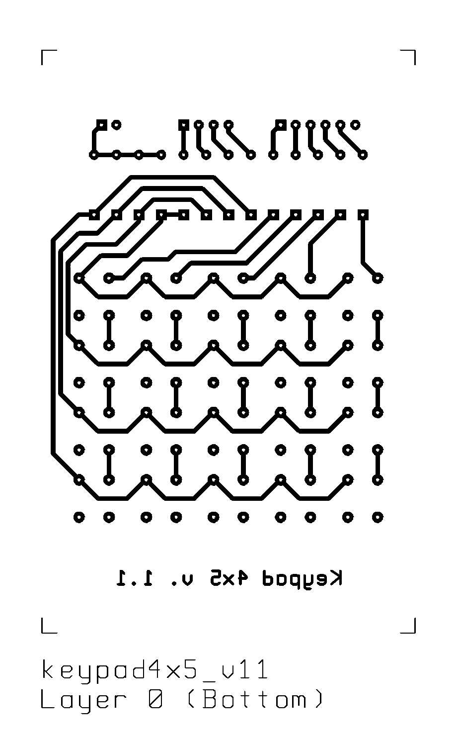 |
Fig. 1 - Components placement and bottom tracks (red, copper side) |
Fig. 2 - Copper side layout at 300 dpi |
 |
|
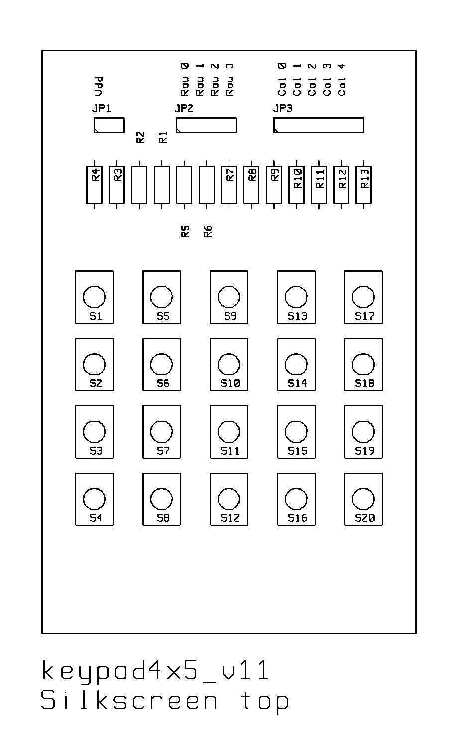
Fig. 3 - Components placement |
 |
| Fig. 4 - Low resolution schematic |
In the end, some details about the circuit I currently use. The keypad is in the full 20 keys version, with PIC's ports RB0-RB3 connected to rows and RC0-RC4 connected to columns. Concerning the cable connecting the keypad and the microcontroller, I use a flat 10 wires cable; the step is 1.27 mm (50 mils), but I have made it suitable to 2.54 mm (100 mils) connectors. A very long and not shielded cable could result in noisy reading; I use an unshielded cable about half a meter long, and, in a normal environment, that is without any particular e.m. interference, my oscilloscope does not show any problem in the waveform on the PIC's I/O pins connected to rows for keypad reading. Hoping I have been useful to you, just to me to wish you a good work! |
| Last update: 20 March 2003, 19.10 |
|